
Part I: Due 30 October, 2000
Part II: Due 6 November, 2000
Part III: Due 15 November, 2000
The purpose of this lab is to have you design the three parts of a computer peripheral: the digital system, the computer interface, and the analog sensory components. The three parts of the lab will each focus on one aspect of the system.
For part I of this lab you will design and implement a state machine that counts events and reports the total number of events within the last minute. This total should be updated at least every 20 seconds.
Your state machine should have the following port declaration:
port( reset: in std_logic;
      clock: in std_logic;
      eventsignal: in std_logic;
      events: out std_logic_vector(7 downto 0) );
To display the output of your system, design a combinational circuit that takes an unsigned 8-bit binary number and displays it as a 2-digit hexadecimal number on the 7-segment displays.
Extensions:
The purpose of this section of the lab is to introduce you to parallel port communication between a digital logic system and a PC. Digital systems that communicate with PCs through the parallel port include printers, scanners, hard drives, tape drives, and network adapters. Parallel port communication is standardized in IEEE standard 1284. A good source for information about the parallel port is the Parallel Port Center.
The specific tasks for this section of the lab are:
Your digital circuit should then hold the character value in a register until it receives another character. The 8 bits in the register should also be outputs of the digital system. Use these outputs (what you receive from the computer) to drive the 8 LEDs on the board.
Test this code by having the Altera chip read eight inputs (e.g. from the DIP switches) and send them to the computer when you press a button. It should not be constantly sending the values, although it can hold the data lines.
The extension for this section of the lab is to integrate parts I and II so that the computer can tell the chip when to reset and can query the chip to get the current event rate/minute.
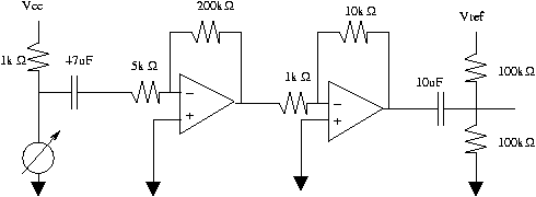
Build/use a sensing and A/D circuit that connects a photosensor with the FLEX chip. The circuit will contain--at least--the transducer, an amplifier stage, and an A/D converter. Then connect together all three components--the A/D system, the digital circuit, and the communications circuit--into a single system that communicates a person's pulse to the computer.
The circuit you want to use will look something like the following:
A circuit like this will be set up on the breadboard in the computer lab. You are free to use it, or you may build your own if you believe you can do better. This circuit has a DC offset removal input stage (hi-pass filter), two amplification stages, and a DC offset stage at the end to move the output back to the range of 0-5V for the A/D conversion.
The analog circuit connects directly to the 0804 A/D converter. The A/D converter should be set up in a free-running mode. The interrupt line outputs a pulse when a new reading is available. You will be able to connect the FLEX chip to the interrupt line and the 8 data lines coming out of the A/D converter. These will be the input to your circuit. You will need to do some simple processing on the signal in order to locate the peaks or valleys. Since this signal will be noisy, you probably want to do some simple averaging combined with hysteresis. Then you want to feed the peak occurances to your event counter.
The end result of this lab should be a system that counts pulses, outputs results in real time on the FLEX board and can communicate this result to the computer. In your event counter, you may just want to count pulses for 10 seconds and multiply by 6 (shift left 1 + shift left 2) to get a per minute signal. To clean it up, then average the last three 10-second readings to get a cleaner signal.
When you have a complete system working, demo it and then write up a lab report on the project as specified below.
Note: the A/D converter will freak out if it receives a significant negative voltage. Turning the system off and back on seems to reset it.
For each part of this lab you will need to demo your working circuit. The behavior of your circuit will determine your grade for parts I and II. Plan to do these demos during the lab periods on the Monday they are due. You will hand in only one writeup for this lab when you are finished with part III.
If you follow standard design procedures, you will have a majority of the writeup for this lab completed. Clarity in your writeups is essential. Convey what you have done in a clear and concise manner, and in sufficient detail that someone else could replicate your work.
In addition to the standard design steps your lab writeup should include the following: